Creaform HandySCAN BLACK Elite PCB Dimensional Inspection Guide
By Marcus O’Neal • 2nd Jan
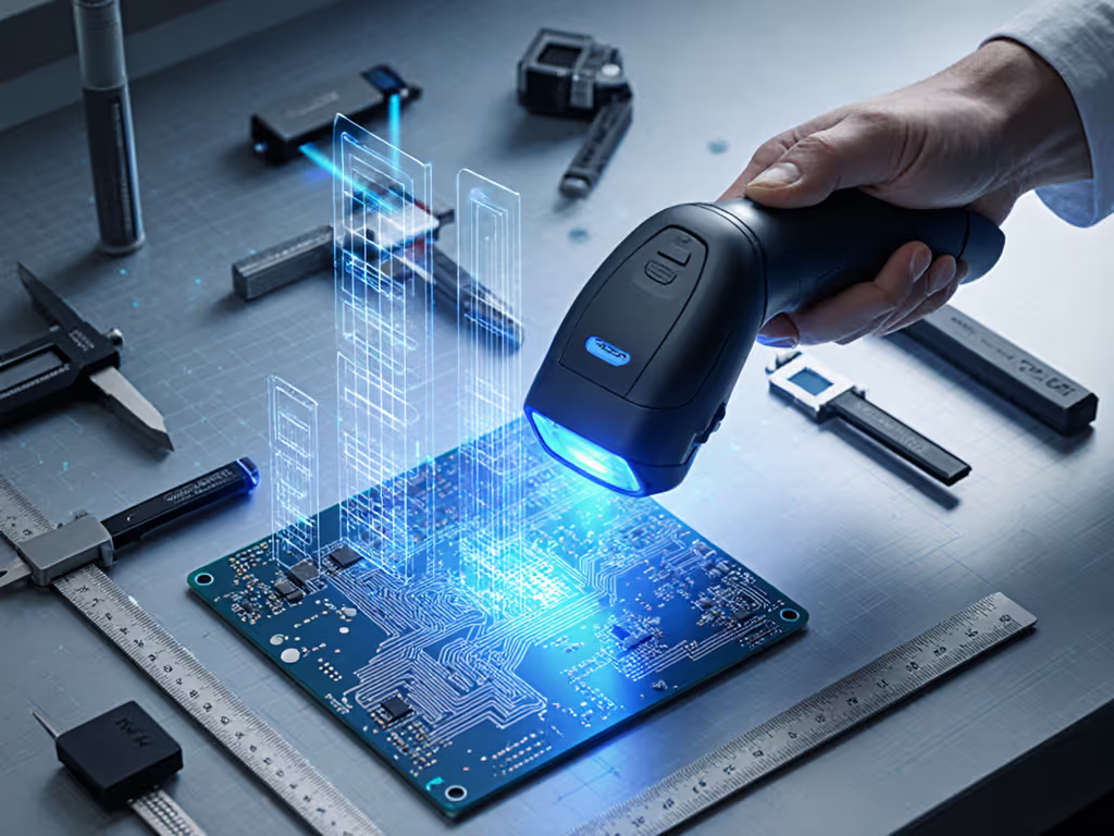
For electronics manufacturing professionals evaluating a handheld 3D scanner for PCB applications, the Creaform HandySCAN BLACK Elite represents a significant advancement in field-deployable metrology. When precision matters, particularly in Creaform HandySCAN electronics workflows where micro-tolerance verification is non-negotiable, this tool delivers metrology-grade accuracy with surprising portability. This guide addresses the critical questions you'll face when integrating 3D scanning technology into your PCB inspection protocol, with emphasis on traceability, uncertainty analysis, and audit compliance. For a quick refresher on the accuracy vs precision distinction, review our guide before setting PCB tolerances.

Why PCB Dimensional Inspection Demands New Approaches
How does traditional PCB inspection fall short for modern electronics?
Traditional coordinate measuring machines (CMMs) require fixturing, environmental control, and trained operators (resources many job shops lack between production runs). Manual calipers and optical comparators succumb to human error during repetitive micro-component measurement tasks. As PCB features shrink and tolerances tighten, these methods become statistically unreliable without rigorous MSA studies that few teams have time to execute properly. To reduce variability at the source, see common measurement error types and how to mitigate them in production.
The moment you're measuring components under 1.0mm pitch or verifying coplanarity within ±0.05mm, uncertainty bites at edges. I've seen countless audit findings where teams used calipers with 0.01mm resolution to verify 0.02mm tolerances, a fundamental violation of the 4:1 test accuracy ratio requirement. The HandySCAN BLACK Elite bridges this gap with metrology-grade validation without shop floor disruption.
What unique challenges does PCB inspection present?
PCB dimensional inspection creates three specific metrology challenges:
- Micro-scale features requiring sub-0.05mm resolution (e.g., 0.4mm pitch components, 0.2mm via holes)
- Mixed reflectivity surfaces where solder mask, copper traces, and component bodies create optical nightmares
- Assembly stack-up tolerances requiring position verification within complex 3D assemblies
Unlike mechanical parts, PCBs introduce thermal warpage risks from solder reflow cycles and environmental sensitivity during measurement. Your scanner must account for both the instrument's uncertainty budget AND the part's thermal behavior during data capture.
Technical Capabilities for Electronic Applications
How does the HandySCAN BLACK Elite handle micro-component measurement?
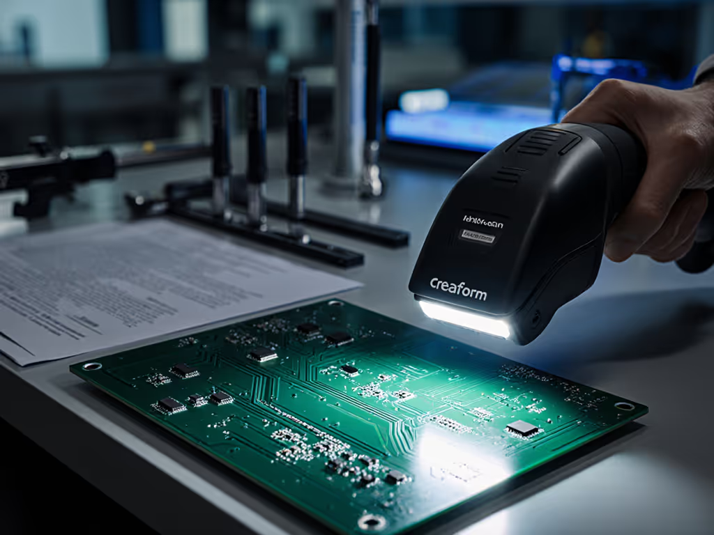
With single-point accuracy of 0.025mm (0.0009") and volumetric accuracy of 0.020mm + 0.040mm/m, this scanner delivers performance that meets ISO 17025 certification requirements for electronics inspection. Crucially, it achieves this without target markers on the PCB itself, a game changer for production environments where adhesive residues could contaminate boards.
The device's 11 blue laser crosses (plus single line mode) overcome the reflectivity challenges inherent in electronic assembly verification:
- Dark solder mask: Blue laser penetrates matte black surfaces where red lasers fail
- Shiny connector leads: Dual camera system compensates for specular reflections
- Component heights: 0.3 m to 2.5 m working distance accommodates populated boards
Importantly, Creaform provides full traceability documentation against ISO 10360 and VDI/VDE 2634 Part 3 standards (not just marketing claims). If traceability fundamentals need a deeper dive, start with our measurement traceability primer. This chain-of-traceability documentation proved critical when an auditor once questioned our measurement environment for a defense contract. We produced the complete calibration history from our lab's reference thermometer to the national metrology institute, and the audit focus immediately shifted from compliance to collaboration.
What's the actual measurement resolution for PCB features?
While specs list 0.025mm resolution, practical micro-component measurement requires understanding four key factors:
| Factor | Impact on PCB Measurement | Mitigation |
|---|---|---|
| Laser wavelength | Critical for dark PCB surfaces | 450nm blue laser penetrates solder mask |
| Point spacing | Must be ≤1/5 feature size | 0.1mm spacing standard; 0.025mm optional |
| Surface reflectivity | Creates data voids | Dynamic exposure adjustment in VXelements |
| Thermal stability | PCB warpage during measurement | Scan within 20-25°C controlled environment |
For 0.4mm pitch components, you need ≤0.08mm point spacing, well within the HandySCAN's capabilities. But remember: specs assume ideal conditions. Your uncertainty budget must include environmental factors. I recommend this minimal PCB scanning checklist:
- Board temperature stabilized within 22±2°C
- Humidity <60% RH to prevent static discharge
- Measurement completed within 15 minutes of environmental stabilization
- Reference calibration performed same day at working temperature
Environmental Control & Uncertainty Analysis
How does temperature affect PCB dimensional inspection?
FR-4 PCB material has a coefficient of thermal expansion (CTE) of approximately 17ppm/°C. This means a 100mm board changes dimension by 0.017mm per 1°C temperature shift, exceeding tolerance for many precision applications. Unlike lab-based CMMs, the HandySCAN BLACK Elite gives you field deployability but demands disciplined environmental management.
Your uncertainty budget must include: Build an audit-ready model using our step-by-step measurement uncertainty budget guide.
Total Uncertainty = √(Scanner² + Environment² + Operator² + Part²)

Where:
- Scanner = 0.025mm (per certificate)
- Environment = (Part CTE × ΔT) + (Scanner CTE × ΔT)
- Operator = <0.01mm with proper training
- Part = Thermal warpage + mounting stress
When verifying medical device PCBAs, I documented a case where 3°C ambient temperature swing introduced 0.05mm warpage in a 150mm board, rendering supposedly "in-tolerance" measurements meaningless. This is why I always say: Trace it, budget it, then trust it under audit.
What's the minimum tolerance you can reliably verify?
The 10:1 rule of thumb applies strictly here. With the HandySCAN BLACK Elite's 0.025mm accuracy, the practical lower tolerance limit is 0.25mm. For tighter tolerances (e.g., 0.1mm coplanarity on BGA packages), you must:
- Reduce environmental uncertainty through strict temperature control
- Apply thermal compensation algorithms in VXinspect software
- Verify critical features with coordinate measurement machine spot-checks
For true sub-0.1mm verification, consider this measurement strategy hierarchy:
Never use a single instrument for tolerances tighter than 4x its expanded uncertainty. For 0.05mm tolerances, you need ≤0.0125mm uncertainty, requiring environmental control beyond most production floors.
Audit Readiness & Documentation
How does the HandySCAN BLACK Elite support ISO 9001/AS9100 compliance?
Unlike many 3D scanners that treat calibration as an afterthought, Creaform builds compliance into the workflow:
- Integrated calibration plate with traceable certificate (NIST or equivalent)
- Daily performance verification protocol documented in software
- VXelements software generates complete measurement reports with uncertainty values
- Full ISO 17025 accreditation for calibration processes
In my audit experience, the difference between a minor finding and a major nonconformance often comes down to documentation depth. When we deployed these scanners across three facilities, we standardized our surface defect detection workflow to include:
- Pre-scan environmental log (temperature, humidity, stabilization time)
- Calibration plate verification with dated certificate
- Reference measurement of known artifact
- Scanned data with uncertainty overlay in reports
- Operator certification documentation
This created complete traceability from measurement to national standards, exactly what auditors expect but rarely see implemented consistently.
What documentation must accompany scan reports for audit purposes?
Your PCB inspection reports should include these non-negotiable elements:
- Equipment ID and current calibration status
- Environmental conditions during measurement
- Software version and analysis parameters
- Uncertainty budget components
- Reference artifact verification results
- Operator certification documentation
- Raw data availability statement
I recall one aerospace audit where the auditor specifically asked for "the thermometer calibration behind your CMM room logs" exactly the kind of question that reveals whether your documentation is truly audit-ready. Teams that treat measurement environment as carefully as they treat instruments earn credibility that smooths the entire audit process.
Implementing PCB Inspection Workflows
How should you structure your MSA for electronic assembly verification?
Your measurement system analysis must account for PCB-specific variables. Here's a lean MSA approach for PCB dimensional inspection:
- Select representative parts: Include boards with dark solder mask, high reflectivity components, and mixed topography
- Document environmental conditions: Measure temperature at scanner, board, and ambient locations
- Standardize scanning technique: Define consistent distance, angle, and speed protocols
- Include known defects: Build golden samples with controlled defects (e.g., 0.05mm lifted lead)
Calculate your Gage R&R with environmental factors included (this is where most teams fail). If your measurement variation exceeds 10% of tolerance (per AIAG guidelines), you must address environmental control before trusting the data.
What workflow integration considerations matter most?
The HandySCAN BLACK Elite integrates with existing quality systems through: If you’re pushing SPC to the edge of the line, these wireless SPC tools can eliminate manual data entry errors.
- VXinspect software exporting to standard formats (STEP, IGES, STL)
- SPC data channels for real-time process control
- Customizable reporting templates matching your organization's requirements
- API access for enterprise system integration
For medical device manufacturers under FDA 21 CFR Part 820, ensure your software validation includes:
- User access controls
- Audit trail functionality
- Data integrity verification
- Change control documentation
Remember that no scanner, even this capable one, replaces proper measurement system design. Your environmental controls, reference standards, and documentation protocols ultimately determine whether your PCB inspection data will withstand audit scrutiny.
Conclusion: Making the Right Choice for Your PCB Inspection Needs
The Creaform HandySCAN BLACK Elite represents a significant advancement in handheld 3D scanner for PCB applications when implemented with metrology discipline. For production environments requiring 0.025mm+ accuracy, it delivers laboratory-grade results without removing parts from the workflow, provided you rigorously manage the uncertainty budget and environmental factors.
Remember that traceability isn't just about the scanner's calibration certificate, it's about documenting the complete measurement environment from ambient conditions to operator technique. When audits come, they'll reward the teams who've built uncertainty transparency into their workflow, not just those with impressive specifications on paper.
For further exploration of PCB measurement systems, request our detailed uncertainty budget template specifically designed for electronics inspection workflows. It includes environmental factor calculators, documentation checklists, and tolerance mapping guidelines that have helped dozens of manufacturers achieve audit-ready measurement processes without slowing production.
Related Articles