Optical Interferometry: Semiconductor Precision & Control
By Greta Lund • 11th Mar
Understanding the Foundation
What is optical interferometry measurement and why does it matter for semiconductors?
Optical interferometry measurement is a fundamental technique in semiconductor manufacturing that detects surface variations and layer thickness by analyzing how coherent light waves interfere after reflecting from different surfaces or interfaces. In semiconductor fabrication, where perfection is measured in nanometers (or even smaller), interferometry has become a cornerstone of process control. Every wafer, mask, or thin film must meet extreme standards of flatness, smoothness, and uniformity to ensure reliable device performance and high production yield. Even the smallest topographical deviation or thickness variation can affect transistor performance, optical alignment, or pattern fidelity. For a deeper dive into metrology choices across wafer, overlay, and film control, see our data-driven semiconductor metrology tools comparison.
The reason this matters operationally is this: optical interferometry measurement provides atomic-scale sensitivity to detect height variations, layer thickness, and refractive index changes. But sensitivity alone isn't enough. What separates a controlled measurement system from a hope-and-wish approach is documentation: controlled setup procedures, environmental limits, revision-tracked work instructions, and evidence that the tool and operator performed as designed.
How does semiconductor precision metrology differ from other measurement approaches?
Semiconductor precision metrology using interferometric methods differs fundamentally from mechanical gauge techniques. A laser interferometer uses the wavelength of light itself as a reference scale, enabling nano-scale and sub-nano-scale measurement accuracy across an extremely wide range. In practical industrial deployments, laser interferometers can achieve measurement ranges of tens of meters with exceptional stability; for example, commercial systems provide stable measurement ranges of up to 80 meters with accuracy of ±0.5 ppm.
The critical distinction: while mechanical tools (calipers, micrometers, dial indicators) are limited by mechanical contacts and inherent friction, light-based methods sidestep contact altogether. This means:
- No probe wear affecting repeatability
- No hysteresis from mechanical linkages
- Atomic-scale resolution without amplification error
- Traceability to fundamental wavelength standards
However, this precision comes with a requirement: environmental control. Temperature stability, vibration isolation, and clean optical surfaces become acceptance criteria rather than nice-to-haves. If your lab temperature swings 5°C during a run, your laser wavelength shifts, and suddenly your nanometer-level data is suspect. That's why the best shops document environmental limits in their SOPs before they run the first part. If your lab supports customer or regulatory audits, review our ISO/IEC 17025 accreditation guide to align procedures and records with audit expectations.
Practical Applications in Semiconductor Manufacturing
Where do laser interferometer applications actually occur on the factory floor?
Interferometric metrology spans the entire semiconductor process chain:
- Wafer flatness and bow measurement after polishing or deposition
- Thin-film thickness control during multilayer growth or coating steps
- Mask and pellicle inspection in lithography
- Overlay and alignment metrology for stepper calibration
- Stage position and vibration monitoring for motion control in exposure tools
Each application has a different tolerance stack and environmental sensitivity. Wafer flatness inspection might tolerate a few fringe shifts from minor thermal drift; alignment metrology on a lithography stepper cannot. The risk note is this: if you're not documenting which application requires which environmental limits, you're running blind. A missing revision callout on your procedure (something as simple as an outdated temperature range) can trigger a stop-ship during PPAP or audit.
I saw this firsthand: a supplier's measurement procedure lacked a current revision on their test instruction. The micrometer calibration was perfect, the measurements were fine, but because no one could prove which version of the procedure was used, the audit flagged it. Three weeks of evidence gathering, a procedure rewrite with version control, and operator retraining. The next audit took twelve minutes on that station, no questions, just signatures. The difference wasn't the tool; it was the controlled language and documented rigor.
Why are nanometer scale measurement techniques necessary, not optional?
Transistor gate lengths, dielectric layer thicknesses, and alignment tolerances in advanced semiconductor nodes operate at nanometer scales. A 50 nm deviation in a 100 nm film thickness is a 50% error, likely to cause electrical failure or reduced yield. This is not theoretical risk; it's production risk.
Nanometer scale measurement using interferometry detects these variations with atomic sensitivity. Modern instruments use multi-wavelength laser sources or tunable swept lasers to combine the high resolution of monochromatic light with an extended measurement range (critical for multi-layer film thickness and topography mapping).
The acceptance criteria for a nanometer-scale measurement system must include:
- Specified resolution (e.g., 0.31 nm with fringe interpolation techniques)
- Documented measurement uncertainty (±X nm at 95% confidence)
- Environmental limits (temperature stability, vibration isolation)
- Calibration interval and traceability to NIST or equivalent
- Evidence links showing which parts were measured under which conditions
If it isn't documented, it's hope, not evidence under pressure.
Environmental Control and System Stability
What environmental control requirements are non-negotiable?
Environmental control requirements are the difference between consistent, auditable measurements and erratic data that fails GR&R. Laser wavelength is stable, but only if the surrounding conditions are controlled:
- Temperature: Thermal expansion of optical components and changes in air refractive index shift measurements. A 1°C change can introduce tens of nanometers of error in long-path interferometry. Most labs specify ±0.5°C or ±1°C stability during measurement.
- Vibration: Mechanical oscillation of the interferometer arm, optical bench, or sample causes fringe instability and prevents coherent signal integration. Isolation tables and structural damping are not luxuries; they are acceptance criteria.
- Optical surface cleanliness: Dust, fingerprints, or condensation degrade fringe contrast and introduce non-linear errors. Controlled handling and storage are procedural requirements.
- Humidity: In some optical designs, moisture absorption in coatings or optical cement can shift refractive index. Documentation of humidity range is essential.
The risk before convenience principle applies here. Yes, you could run measurements in an uncontrolled area and save facility costs. But your data becomes unrepeatable, audit risk climbs, and scrap typically follows. Environment control is not optional; it is foundational to measurement system validity.
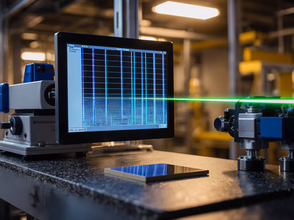
How do heterodyne and swept-wavelength approaches improve stability?
Historically, laser interferometry relied on homodyne detection (a single coherent beam split and recombined). Modern systems employ heterodyne methods and wavelength-swept techniques to suppress systematic errors. In heterodyne interferometry, two closely spaced optical frequencies are generated using dual-frequency lasers. Unlike homodyne methods, which use amplitude-modulated signals, heterodyne interferometry utilizes frequency-modulated signals, effectively suppressing the influence of DC drift.
Wavelength-swept approaches go further: by scanning across multiple wavelengths and analyzing the phase shift, systems eliminate periodic nonlinear errors arising from mixed-frequency effects and polarization crosstalk. Recent research demonstrates heterodyne interferometers achieving picometre-level displacement sensitivity with twice the thermal stability of commercial instruments and no detectable periodic errors.
Why does this matter operationally? Fewer systematic errors mean smaller uncertainty budgets, tighter tolerance margins, and higher confidence in pass/fail decisions. To formalize these gains, build a rigorous measurement uncertainty budget tailored to your interferometry setup. When your uncertainty is controlled and documented, your auditor's uncertainty decreases, and so does yours.
Audit Readiness and Documentation
How does wafer flatness measurement fit into a compliant quality system?
Wafer flatness measurement is a critical control point in PPAP submission and ongoing production. Using interferometry, flatness is measured by scanning the wafer surface and reconstructing the height profile with sub-micrometre resolution. But the measurement data alone is not sufficient.
Audit readiness requires:
- Procedure with revision history showing all approved changes
- Calibration certificate for the interferometer, with traceability path and next due date
- Environmental log for the test date (temperature, humidity, operator name)
- Measurement data (not just the Pass/Fail summary, raw fringes or height map if audit logic demands it)
- Acceptance criteria, explicitly linked to design or process specification
- Evidence links connecting measurements to part serial numbers and production lot codes
When an audit arrives, a complete dossier answers every question in the first minute. When documentation is scattered or incomplete, the auditor digs deeper, and surprises emerge. Consistency and documentation convert good measurements into reliable decisions that hold up under scrutiny.
What records must survive a compliance audit?
In ISO 9001, AS9100, IATF 16949, or ISO/IEC 17025 environments, these records are non-negotiable:
- Tool calibration certificates with uncertainty statements, traceability, and dates
- Measurement procedures with revision control and approval signatures
- Environmental monitoring logs (temperature, vibration data if critical)
- GR&R (Gage R&R) study results showing the measurement system is capable
- Raw measurement data linked to part identifiers and batch codes
- Corrective action records if measurement drift is detected
- Operator training records with competency sign-offs
One missing revision callout on a work instruction can flag the entire data set as uncontrolled. Plan for this before the first measurement, not after the audit letter arrives.
Resolution, Accuracy, and Uncertainty
What is the difference between resolution and measurement accuracy?
This distinction trips up many teams. For clear examples and pitfalls, see accuracy vs precision. Resolution is the smallest division a tool can display; accuracy is how close that reading is to the true value. A laser interferometer might display 0.31 nm resolution (using fringe interpolation techniques), but its measurement accuracy might be ±2 nm or larger, depending on wavelength stability, environmental drift, and calibration traceability.
Accuracy is what you need for process control. Resolution is marketing. When comparing tools or justifying an upgrade, ask for accuracy and uncertainty budget, not resolution. If a vendor emphasizes resolution without addressing uncertainty, that's a red flag.
How do you set measurement tolerance and select the right tool class?
The guidance is the 10:1 test accuracy ratio (TAR): your measurement uncertainty should be no more than 10% of the part tolerance being inspected. For a step-by-step framework that maps tolerance to tool capability, use our tool selection by tolerance guide. For tighter control (e.g., critical safety or aerospace), a 4:1 ratio is preferred. If your wafer flatness tolerance is 100 nm, you need a system capable of ±10 nm or better (10:1 ratio).
Once you know your tolerance and required uncertainty:
- Define the measurement task (flatness, thickness, overlay, vibration monitoring)
- Calculate the tolerance window and required uncertainty (using 10:1 or 4:1 rule)
- Match tool capability to that uncertainty, consider environmental factors, calibration interval, and system drift
- Document acceptance criteria in your procedure
- Plan environmental controls and log them during use
Oversizing tools (buying a ±0.5 nm system when ±20 nm is sufficient) wastes capital and ties up lab space. Undersizing creates audit risk and scrap. The right choice is the tightest tool that meets your tolerance with margin and is sustainable in your environment.
Moving Forward
Optical interferometry is the gold standard for semiconductor metrology because it offers nanometer sensitivity, traceability to wavelength standards, and freedom from mechanical wear. But that capability is only valuable if it's controlled, documented, and integrated into your quality system.
The next steps are to audit your current measurement procedures for completeness: Are environmental limits specified? Are calibration intervals current? Do your work instructions include revision numbers and operator sign-off? If not, update them before your next audit or PPAP. Run a GR&R study on your interferometry measurement system to prove it's capable. Establish a log linking environmental conditions to each measurement.
For teams new to interferometry, partner with a metrology service lab or instrument vendor to validate your setup and train operators on proper technique (beam alignment, surface cleanliness, environmental isolation). Invest in operator training and make it repeatable. The ROI is lower scrap, fewer audit findings, and the quiet confidence that your measurements can defend any decision under pressure.
Consistency and documentation convert good measurements into reliable decisions. Start there.
Related Articles